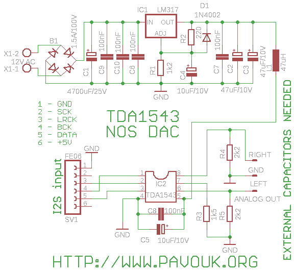
Like a simplier variant of DAC I used well-established cheap circuit TDA1543A, which is easily available for me. His paper parameters are not nothing special, but DAC allow running without oversampling and his sound is surprisingly good. It's possible to enhance them with parallel connection of more pieces of these circuits, which I made on 10xTDA1543 PCB. DAC has consumption about 50mA and with supply voltage 8V it's needed to cool them. Advantage of NOS - non over sampling DACs is theoretically more natural sound, because with oversampling process are added sound components which was not in original audio signal. DAC without low-pass filter relies on that that filtering of sample frequency will be next in the audio chain. Most often in the loudspeakers and human ears.
In supply section after bridge rectifier and smoothing capacitor is used common voltage regulator LM317, which has with R1 and R2 adjusted output voltage about 8V. Supply line goes through inductor to DAC chip for theoretically lower HF interference which goes on the power lines.
DAC has current outputs which are converted to the voltage output with the aid of resistors R4 and R5. Sometimes is used circuit with operational amplifiers combined with low-pass filter which is much complicated and can introduce distortion in to the sound. Low-pass filter which is used for removing sampling frequency unfortunately introduce distortion on high frequencies. Sound is then more flat. Because DAC doesn't have symmetrical power supply, that we must use capacitors in series with the outputs. It's desirable to use high quality capacitors with sufficient capacity. It's not recommended to use electrolytic capacitor. I used foil capacitors with 10uF value which are connected between outputs and output connector. They are placed out of board and they are not drawed in a schematics diagram. Output must not be too much loaded and should be connected to input of preamplifier or power amplifier with input impedance at least 10 kiloohms.
It's possible to have separated supply for DAC from independent winding of power transformer for better isolation between S/PDIF decoder and dac with changing voltage. We can use board for building of stack, where are integrated circuits placed directly one on another with small heat sinks between them. With this connection we must change values of resistors R3, R4 and R5, where with using 10 circuits we use ten times lower values - 150R, 220R and 220R. We must add small heat-sink to LM317 regulator. Transformer must be dimensed for current 0.5A.
We are placing components on board from smaller to bigger. We begin with SMD components and next with normal parts. We must mount small heat-sink on the DAC otherwise it overheats and it can burns (my own experience). For I2S connector we can use jumper ribbon with pins or sockets. It depends on that how we want to mechanically connect DAC with S/PDIF decoder together. I used on both sides pins and for board conection I soldered two sets of 6pin sockets together.
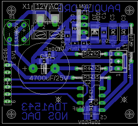
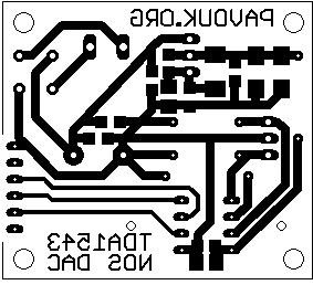
Printed circuit board is designed with only one side. It allows to create him in amateur conditions. SMD components are placed from a bottom side and components with terminals and connectors are mounted from top side. There are holes for heat-sink fixing and for mounting board with screws.
We must set the right data format with jumpers on a S/PDIF decoder board. Circuit TDA1543 use I2S data format. Circuit TDA1543A use 24-bit right-justified data format.


| Name | Value and type | quantity |
|---|---|---|
| R1 | 1k2 SMD1206 | 1x |
| R2 | 220R SMD1206 | 1x |
| R3 | 1k5 | 1x |
| R4-R5 | 2k2 | 2x |
| C1 | 4700uF/25V electrolytic | 1x |
| C2-C3 | 47uF/10V SMD tantal size C | 2x |
| C4-C5 | 10uF/10V SMD tantal size B | 2x |
| C6-C10 | 100nF SMD1206 ceramic | 5x |
| Cext | 10uF foil | 2x |
| IC1 | LM317T | 1x |
| IC2 | TDA1543(A) | 1x |
| J1 | Molex 3pin | 1x |
| L1 | 47uH axial | 1x |
| D1 | Diode 1N4007SMD MELF | 1x |
| B1 | Bridge rectifier 1.5A/100V | 1x |
| SV1 | Jumper ribbon 6 pins | 1x |
| X1 | Frame terminal AK300/2 | 1x |
Circuit diagram of this DAC is very simple and with careful work and right setting of S/PDIF decoder it must works on the first switch-on. Don't forget connect outputs over capacitors Cext. I build this DAC like a simpliest variant of DAC for verification functionality of S/PDIF decoder and his sound is surprisingly good.
 English
 Česky
Česky