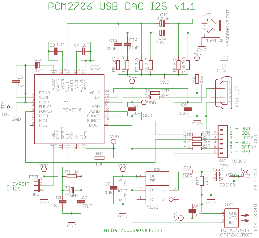
I already built a couple of USB DACs but no one have I2S output. Some people doesn't need S/PDIF input and they want only USB. With these requirements is unnecessary to convert signal first from USB to S/PDIF and next to I2S for DAC. This board have analog headphone output, electric galvanically isolated S/PDIF output and optical TOSLINK. After switching jumper circuit switch to I2S mode, which can be directly connected to DAC.
Diagram use PCM2706 circuit from Texas Instruments. Circuit includes Digital/Analog converter, S/PDIF output, I2S output and HID interface for push buttons. Schematics diagram is similar to recommended diagram in datasheet. USB input has standard miniUSB connector. Circuit PCM2706 has integrated headphone amplifier and his output goes through external low-pass filter to standard 3.5" jack socket. Circuit includes digital volume control in a range 0dB to -64dB with 1dB step. This control works only with analog output. It doesn't have effect for I2S and S/PDIF outputs. In S/PDIF mode (FSEL=1) is active S/PDIF data output and on pins FUNC0 to FUNC3 are inputs for push buttons, which are not used. S/PDIF output goes to optical transmitter and to RS485 driver which boosts signal to voltage divider which divide signal approximately to 1 volt and adjust output impedance to about 75 ohms. Signal is galvanically isolated by pulse transformer.
In I2S mode (FSEL=0) goes to the DOUT data in I2S format (16 bits left justified) and on pins FUNC0 to FUNC2 are LRCK, BCK and SYSCK signals. On the pin FUNC3 is now I2S data input signal which is connected to the internal DAC. In my circuit is only on the testpoint and headphone output is silent in this mode. If you want to have active this output in I2S mode, that you can connect it with DOUT. This functionality is described for use with sound effects with external DSP. I2S output is not isolated that if you want them galvanically isolate you must use external isolator.
Schematics should work with PCM2707 circuit too, because I keeped all connection requirements for both chips. This was not tested because I hadn't this chip available.
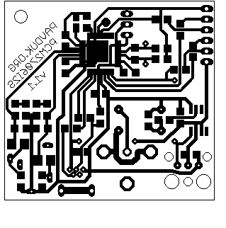
We place components on the board from smaller to bigger. We begin with integrated circuits and next continue with other SMD components. Next we continue from a top side with wire wraps and other components. Last we assemble connectors. If you don't want to use for example analog output, that you don't need assemble parts of analog filter and jack connector. If you don't want electrical S/PDIF output that don't assemble IC2, R16, R17, TR1 and X3. Optical output includes only C9 and OX1.
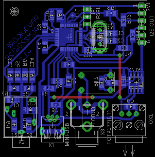
Printed circuit board is single-sided which allows to create him in amateur conditions. SMD components are from a bottom side and parts with wires, wire wraps and connectors from a top side. Board dimensions was changed a little in a 1.1 version for direct connection with DAC boards. It allows to have connectors on a back panel with boards in one line.
We setting up board only with one jumper JP1. In the zero position is circuit in I2S mode and in the position 1 is in S/PDIF + TOSLINK + headphone output mode.


| name | value and type | quantity |
|---|---|---|
| R1 | 1M SMD1206 | 1x |
| R2, R11 | 1k5 SMD1206 | 2x |
| R3-R4, R12-R15 | 22R SMD1206 | 6x |
| R5-R6 | 16R SMD1206 | 2x |
| R7-R10 | 3K3 SMD1206 | 4x |
| R16 | 360R SMD1206 | 1x |
| R17 | 91R SMD1206 | 1x |
| C1-C2 | 22pF SMD1206 | 2x |
| C3-C9 | 1uF SMD1206 | 7x |
| C10 | 10uF/16V SMD tantal size A | 1x |
| C11-C12 | 100uF/6.3V SMD tantal size B | 2x |
| C13-C14 | 22nF SMD1206 | 2x |
| IC1 | PCM2706 | 1x |
| IC2 | 75176 SMD | 1x |
| JP1 | jumper ribbon 3 pins | 1x |
| OX1 | TOTX177(F,T) Toshiba, GP1FAV31TK0F SHARP | 1x |
| Q1 | 12MHz crystal mini | 1x |
| SV1 | jumper ribbon 6 pins | 1x |
| TR1 | pulse transformer S22083, PE-65612, DA102C | 1x |
| X1 | miniUSB socket USB PCB MBW | 1x |
| X2 | 3.5" socket EBS35 | 1x |
| X3 | cinch socket to PCB TOBU3 | 1x |
Circuit works with the first power-up. Functionality of headphone output, electrical S/PDIF and optical TOSLINK and after switching I2S output was successfully tested.
 English
 Česky
Česky