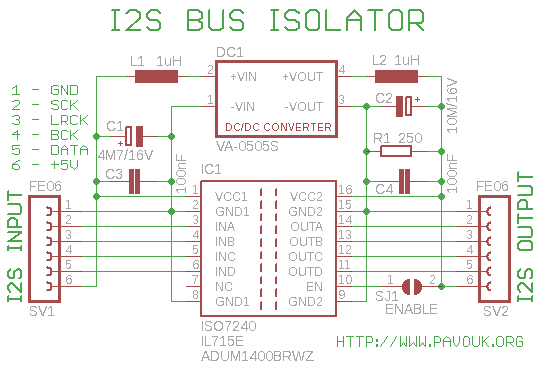
To avoid hum and interference in our high quality DAC we need to galvanically isolate him from a signal source and break potential unwanted ground loop. One possibility is to isolate DAC on input of the S/PDIF decoder with pulse transformer or connect him with optical TOSLINK. When we want to connect DAC directly from USB receiver via I2S bus, that we must use special integrated circuit which works like electrical isolator of TTL signals.
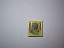
Circuit use specialised circuit IL715E which have on the one side four TTL inputs and on the opposite side corresponding outputs. It perfectly fits to I2S bus, where we have DATA, BCK, LRCK and SCK signals. Circuit requires dual supplying, one on the input and second on the output side. On the input is supply connected to +5V which I bring out them on the I2S connector for future use. Secondary side is supplied from small DC/DC converter. According to recommendations are around converter inductors L1 and L2 and filter and block capacitors. Their values correspond to changer from Aimtec company but probably parts will be acceptable for changers from other companies. For reliable function of converter is on the secondary side load resistor R1 which guarantee minimal current consumption about 20mA. Datasheet have informations about maximum data rate 100Mbps which is far away from our sample frequency 48kHz, where frequency of BCK is 3.072MHz and SCK is 12.288MHz with 4x oversampling. Circuit should work with 192kHz/24bit samples where frequency of SCK is higher 49.152MHz. DAC without oversampling doesn't use SCK signal that we must care only maximal BCK frequency. It is possible to use isolators from other vendors with same pinout, but we must check their maximum data rate and if they doesn't need ENABLE signal.
First we solder integrated circuit and next other SMD components. Last we solder converter and converter from the other side. We must be careful for right orientation of circuit and changer and right polarity of capacitors. If we use circuit which requires ENABLE signal on the pin 10 that we join SJ1.
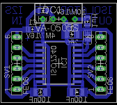
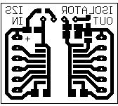
PCB is designed single-sided. Be careful that board is placed between decoder and DAC board up side down. It means that SMD components from a bottom side will be visible up and socket ribbons will be connected to the pins of neighbor boards. First version of board, which I designed had components on the side, where is big filter capacitor on a DAC board, that it was not possible to directly plug board to the neighbours. This version of board has components on the opposite side that it doesn't collide with parts on the DAC board. It is possible to use right angle connectors where we will not have troubles with space, but boards will need much place.
 PDF format
Eagle5 format
OLD version PCB in Eagle5
PDF format
Eagle5 format
OLD version PCB in Eagle5


| name | value and type | quantity |
|---|---|---|
| R1 | 250 (240) SMD1206 | 1x |
| C1 | 4.7uF/16V SMD tantal size A | 1x |
| C2 | 10uF/16V SMD tantal size A | 1x |
| C3, C4 | 100nF SMD1206 ceramic | 2x |
| DC1 | Aimtec AM1S-0505SZ or similar | 1x |
| IC1 | ISO7240, IL715E, ADUM1400BRWZ 0.3" SOIC16 | 1x |
| L1, L2 | 1uH SMD L2012C | 2x |
| SV1, SV2 | socket ribbon 2.54mm 6 pins | 2x |
I tested this circuit with PCM2706 USB board and AD1865 DAC and everything works perfectly to my expectations.
 English
 Česky
Česky