![]() This article descripts, how I built amplifier from Mr. Marshall Leach known
like "The Leach Amp". I built amplifier from the original instructions on these
pages:
http://users.ece.gatech.edu/~mleach/lowtim/. Article about bulding
of this amplifier I found later in journal
A_Radio Praktická elektronika 11/2002. For many years I looked for
construction of HiFi amplifier wit a good parameters, enough power reserve
and simple construction. I built a couple of amplifiers with integrated
circuits MBA810, TDA2005, LM3886, but I was disappointed by their output
quality and noise. I decide to built a classic construction with discrete
components and bipolar transistors. Construction from Mr. Dudek was interesting,
but I didn't like used components and complexity. All of my requirements
satisfied construction of the Leach Amp. Circuit author publicates in a February
1976 in american journal. From these days circuit was not practically changed.
Little changes are descripted on authors page.
This article descripts, how I built amplifier from Mr. Marshall Leach known
like "The Leach Amp". I built amplifier from the original instructions on these
pages:
http://users.ece.gatech.edu/~mleach/lowtim/. Article about bulding
of this amplifier I found later in journal
A_Radio Praktická elektronika 11/2002. For many years I looked for
construction of HiFi amplifier wit a good parameters, enough power reserve
and simple construction. I built a couple of amplifiers with integrated
circuits MBA810, TDA2005, LM3886, but I was disappointed by their output
quality and noise. I decide to built a classic construction with discrete
components and bipolar transistors. Construction from Mr. Dudek was interesting,
but I didn't like used components and complexity. All of my requirements
satisfied construction of the Leach Amp. Circuit author publicates in a February
1976 in american journal. From these days circuit was not practically changed.
Little changes are descripted on authors page.
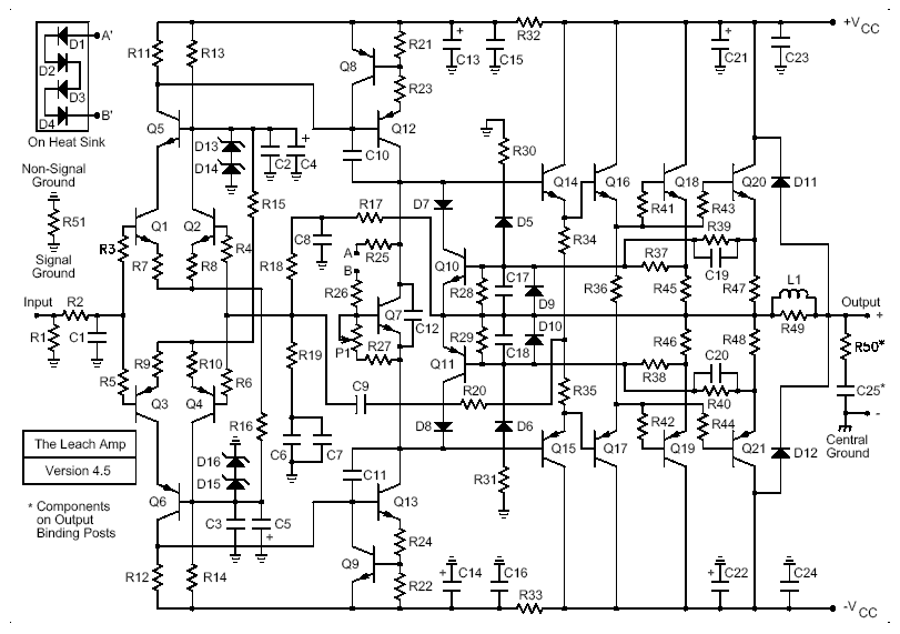
Link to original schematics diagram: http://users.ece.gatech.edu/~mleach/lowtim/graphics/ckt.pdf
Local copy: ckt.pdf
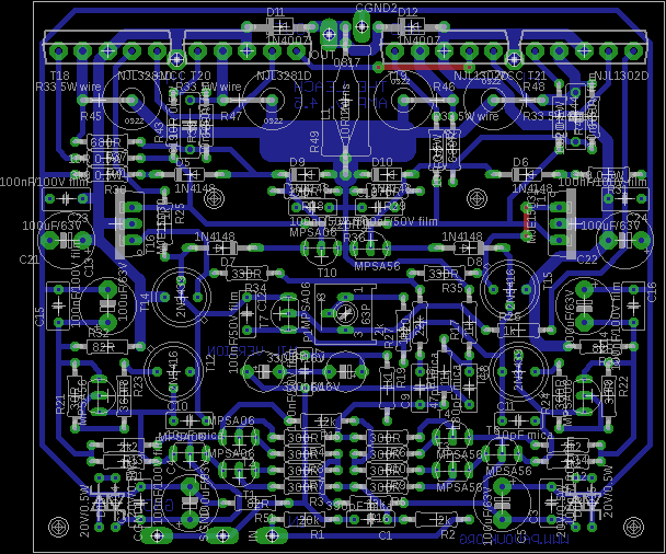
Redrawed schematics diagram for use with NJL transistors with added component values:
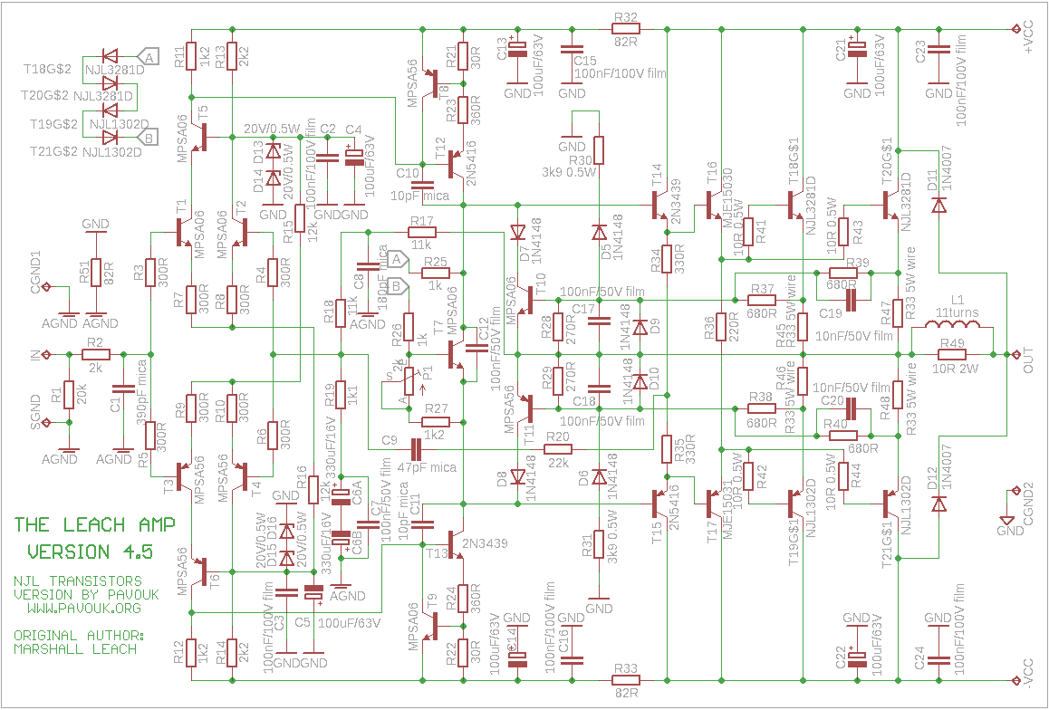
Schematics in Eagle5 format: leachamp4_5.sch
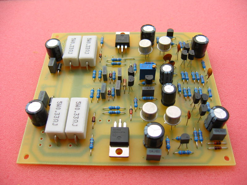
I succeeded to find almost all original components on our local market, which was a miracle. Only a bigger problem was a power transformer and filter capacitors. Recommended toroid transformer for power 200W to 4 ohms is 230V/2x 42V. I succeeded to find in a GM Electronic a toroid transformer 2x36V, 300W. Output power will be a little lower, but for home use it will be more than enough. Voltage after rectification and filtering without load will be about +51V and -51V. I couldn't find capacitors with a 10000uF or 20000uF for 75V. I decided to buy electrolytic capacitors 4700uF/63V and place four pieces parallely on positive voltage and 4 on negative voltage. I was thinking about other option to place 3 pieces of 6800uF/63V on power lines. Mica capacitors are not available at all. I used ceramic instead. Someone said, that ceramic capacitors can "play", but I didn't found any problems. Carbon resistors are allegedly better for Hifi because lower noise, but I hear it after I buyed metalised resistors. I used normal electrolytic capacitors, but probably LowESR types will be better. Power transistors are not original Motorola, or today ON semiconductor, but I didn't found any problem.
| number | name | value |
|---|---|---|
| Transistors | ||
| 12x | Q1, Q2, Q5, Q7, Q9, Q10 | MPSA 06 |
| 10x | Q3, Q4, Q6, Q8, Q11 | MPSA 56 |
| 4x | Q13, Q14 | 2N 3439 |
| 4x | Q12, Q15 | 2N 5416 |
| 2x | Q16 | MJE 15030 |
| 2x | Q17 | MJE 15031 |
| 4x | Q18, Q20 | MJ 15003 (NJL3281D) |
| 4x | Q19, Q21 | MJ 15004 (NJL1302D) |
| Diodes | ||
| 12x | D1, D2, D3, D4, D11, D12 | 1N4007 |
| 12x | D5, D6, D7, D8, D9, D10 | 1N4148 |
| 8x (15x) | D13, D14, D15, D16 | 20 V Zener +5% tolerance, 0.5W |
| Capacitors | ||
| 2x | C1 | 390 pF mica |
| 14x | C2, C3, C15, C16, C23, C24, C25 | 100nF/100V film |
| 8x | C7, C12, C17, C18 | 100nF/50V film |
| 12x | C4, C5, C13, C14, C21, C22 | 100uF/63V radial electrolytic |
| 2x (4x) | C6a, C6b | 220uF/16V bi-polar electrolytic (4x 330uF/16V) |
| 2x | C8 | 180pF mica |
| 2x | C9 | 47pF mica |
| 4x | C10, C11 | 10pF mica |
| 4x | C19, C20 | 10nF/50V film |
| Rezistors | ||
| All resistors are 1% carbonic or metalised 0,5W if not noted otherwise | ||
| 2x | R1 | 20 kohm |
| 2x | R2 | 2 kohm |
| 16x | R3, R4, R5, R6, R7, R8, R9, R10 | 300 ohm |
| 6x | R11, R12, R27 | 1.2 kohm |
| 4x | R13, R14 | 2.2 kohm |
| 4x | R15, R16 | 12 kohm |
| 4x | R17, R18 | 11 kohm |
| 2x | R19 | 1.1 kohm |
| 2x | R20 | 22 kohm |
| 4x | R21, R22 | 30 ohm |
| 4x | R23, R24 | 360 ohm |
| 4x | R25, R26 | 1 kohm |
| 4x | R28, R29 | 270 ohm |
| 4x | R30, R31 | 3.9 kohm 1/2 W |
| 6x | R32, R33, R51 | 82 ohm |
| 4x | R34, R35 | 330 ohm |
| 2x | R36 | 220 ohm |
| 8x | R37, R38, R39, R40 | 680 ohm |
| 8x | R41, R42, R43, R44 | 10 ohm 1/2 W |
| 8x | R45, R46, R47, R48 | 0.33 ohm 5 W wire-wound |
| 4x | R49, R50 | 10 ohm, 2 W |
| Other | ||
| 2x | P1 | 2 kohm more turn cermet trimmer |
| 1x | T1 | Toroid power transformer SEC 2x40V AC 300W |
| 8x | C1P, C2P | 4700uF/63V (6x 6800uF/63V 4x 10000uF/63V) |
| 8x | C3P | 100nF/200V |
| 1x | D1P | Bridge rectifier 35A/200V |
| 5x | Fuse casing | |
| 1x | F1 | Fuse 3.15A T |
| 4x | F2, F3, F4, F5 | Fuse 5A F |
| 8x | Insulative bed under transistors + screw insulatives 16x | |
| 20x | Solder eye M4 | |
| 2m | Shrinking spaghetti 4mm | |
To prevent DC offset problems is needed to match transistors Q1-Q4 and zener diodes. In original article is a deep description how to do it. With transistors I had not any problems at all. Probably today is their producing more precise, when they are from identical series. With zener diodes it is worse. We connect 20V zener diode in a series with a resistor on the voltage power supply that to set diode current to a 3.3mA. I discovered, that zener voltage changing according to temperature and term of connection to voltage. During measuring I tried to keep identical conditions for all diodes and I waits for steady of value after about 1 minute. I buyed more zener diodes and every piece I measured three times and write down their values. After measuring I collected diode pairs for match voltages on each board.
 Next was needed to wind L1 around R49. First I doesn't know which select
wire and how their best wind on the resistor. I used lacquered wire from
output inductor from an old PC power supply with diameter about 1mm.
I wounded 11 turns on a screwdriver with a similar diameter like a R49.
Finished inductor I placed on R49, turn their ends and solder them on the
resistor terminals. Resistor with an inductor is normally soldered to
board.
Next was needed to wind L1 around R49. First I doesn't know which select
wire and how their best wind on the resistor. I used lacquered wire from
output inductor from an old PC power supply with diameter about 1mm.
I wounded 11 turns on a screwdriver with a similar diameter like a R49.
Finished inductor I placed on R49, turn their ends and solder them on the
resistor terminals. Resistor with an inductor is normally soldered to
board.
 I used original circuit board layout version 4.5 which looks perfectly
suitable. Circuit board is one sided, nice symmetrically designed and all
components fits to them perfectly. Only one little problem was small solder
spots. It's not possible to drill a little bigger holes. First piece of
circuit board I redrawed to an Eagle and consequently plot it on cuprextit
and etch it. Next I leave them to make at Mr.
Kohout which makes simple circuit
boards by photo path. I only tell him page, where was circuit board published
in Aradio magazine. Concretly "Praktická elektronika A Radio - 11/2002 page 13".
Because he already had film negative, that curcuit board was cheaper.
Circuit board was varnished to prevent oxidation and better soldering.
Before assembling is suitable to check, that all holes are sufficient for
components and wires. When I increased hole on an assembled board, I little
damaged a case of one electrolytic capacitor.
I used original circuit board layout version 4.5 which looks perfectly
suitable. Circuit board is one sided, nice symmetrically designed and all
components fits to them perfectly. Only one little problem was small solder
spots. It's not possible to drill a little bigger holes. First piece of
circuit board I redrawed to an Eagle and consequently plot it on cuprextit
and etch it. Next I leave them to make at Mr.
Kohout which makes simple circuit
boards by photo path. I only tell him page, where was circuit board published
in Aradio magazine. Concretly "Praktická elektronika A Radio - 11/2002 page 13".
Because he already had film negative, that curcuit board was cheaper.
Circuit board was varnished to prevent oxidation and better soldering.
Before assembling is suitable to check, that all holes are sufficient for
components and wires. When I increased hole on an assembled board, I little
damaged a case of one electrolytic capacitor.
Original printed circuit board with heatsink drilling: http://users.ece.gatech.edu/~mleach/lowtim/graphics/layouts.pdf
Local copy:layouts.pdf
Rearranged PCB for direct assembling NJL transistors. I had to make smaller PCB than original thanks to limited Light version of Eagle, but I hope that it is OK.
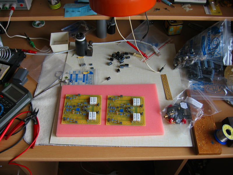 It's good to begin assembling of circuit board from the smallest components
to largest. First I soldered short-circuit jumper. Next I assembled all small
resistors and after them diodes. I checked resistor values and diode polarity
with a multimeter before assembling. Next I assembled small capacitors
and smallest, middle and largest transistors. Specially I doublechecked
their position. There remaining only big resistors and electrolytic capacitors,
where I specially check polarity. It's needed to right turn pins on Q16 and Q17
in line with hole position and thickness of small heat sink.
It's good to begin assembling of circuit board from the smallest components
to largest. First I soldered short-circuit jumper. Next I assembled all small
resistors and after them diodes. I checked resistor values and diode polarity
with a multimeter before assembling. Next I assembled small capacitors
and smallest, middle and largest transistors. Specially I doublechecked
their position. There remaining only big resistors and electrolytic capacitors,
where I specially check polarity. It's needed to right turn pins on Q16 and Q17
in line with hole position and thickness of small heat sink.
I couldn't find suitable heat sink for a long time. I found perfect profile
at small vendor, but it was much shorter than I needed it.
Finally I obtained contact on a company ALUPA,
which has in their list aluminium profile which fits exactly for our
amplifier. Profile has marking
ZH-2476.
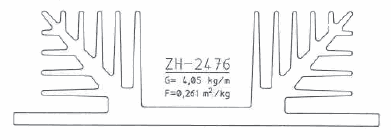 Unfortunately I doesn't know exactly required size, that I had to cut them
with a circular saw, which going very badly, because aluminium "flows".
Finally I cut heat sink to lenght 15cm and drilled to them holes according to
original PDF document by 4mm drill except diodes. Holes for diodes I drilled
to their tight contact with heat sink.
Collector of power transistors I connected from upper side with help of solder
eye and thick wire. I drilled holes for wires between transistors, but it was
not a good idea, because I had to a little nibble mica beds. Better will be to
make holes on the side of transistors.
Unfortunately I doesn't know exactly required size, that I had to cut them
with a circular saw, which going very badly, because aluminium "flows".
Finally I cut heat sink to lenght 15cm and drilled to them holes according to
original PDF document by 4mm drill except diodes. Holes for diodes I drilled
to their tight contact with heat sink.
Collector of power transistors I connected from upper side with help of solder
eye and thick wire. I drilled holes for wires between transistors, but it was
not a good idea, because I had to a little nibble mica beds. Better will be to
make holes on the side of transistors.
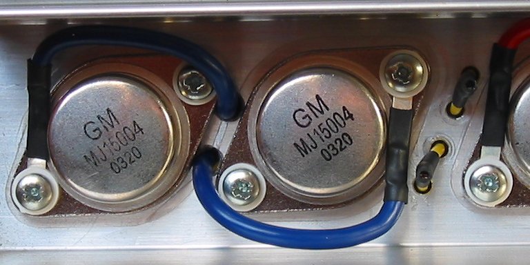
Transistors are attached this way: First I spread his inner side with a thin layer of silicon vaseline. Next I attached on them mica bed. Next I soldered two thicker wires long 10cm, attached a piece of shrinkage spaghetti and shrink with lighter. Wires to collectors must be longer for about 5cm. Next I spreaded mica bed from the other side too. Layer must be very thin, because vaseline tried to push out. Finally I gave transistor on his place on the heat sink, in to the holes I placed screw isolant, under one I gave solder eye with soldered thicker wire and I screw up M3 15mm screws. In to the heat sink I placed and solder up 4 diodes according to original document and I drop them with glue. I drilled a small holes in a corners of the heat sink and I made worm with a M3 screw-cutter. I placed 5mm M3 spacer leg. For better heat removal is good to place blacked heat sink vertically, but I was limited by space and technological possibilities. However I didn't see any problems with overheating.
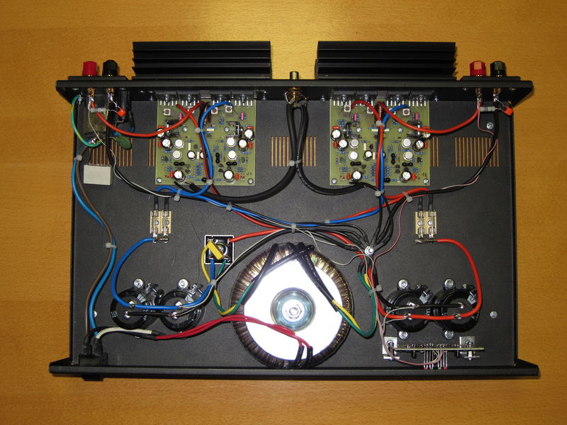
 In construction I comes again from
original organization. I had available old casing from some device
with height 12cm, width 48cm and depth 25cm. On the front panel is placed only
power switch and four diodes. Two for positive and negative supply and two for
clipping indicator of the left and right channel.
Front panel from aluminium I polished, that now it looks almost like a mirror.
On them is placed logo made from cuprextit and glued with both sides sealing
tape. But it doesn't look much good.
In construction I comes again from
original organization. I had available old casing from some device
with height 12cm, width 48cm and depth 25cm. On the front panel is placed only
power switch and four diodes. Two for positive and negative supply and two for
clipping indicator of the left and right channel.
Front panel from aluminium I polished, that now it looks almost like a mirror.
On them is placed logo made from cuprextit and glued with both sides sealing
tape. But it doesn't look much good.
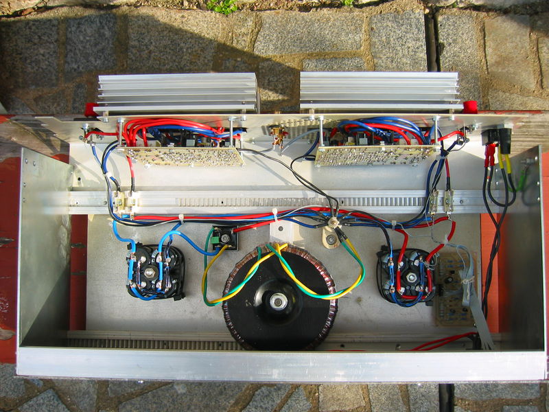
Toroid transformer is placed in a center close to front panel far from electronics due to interference reason. He is attached with a bigger screw to base of the chassis. Nearby is central isolated ground point and bridge rectifier. Protective ground wire is connected from the power plug to the metal chassis. Ground from plug is not connected with a central amplifier ground for preventing ground loops and interference problems.
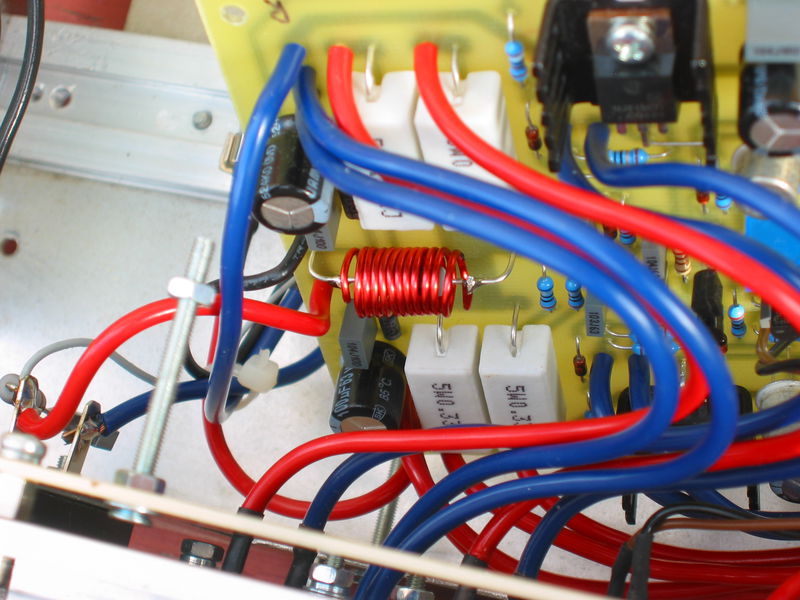
On the left and right side from the transformer are located filter capacitors placed vertically. Between them is longer screw with a female screw and plastic hose for preventing of wearing through capacitor insulation. On the top of the screw is placed bigger rubber pad with a female screw. Capacitors are binded together. Strong power wires are from one piece of wire and goes from rectifier over all filter capacitors to fuse holders. Maybe is better to connect all capacitors with same long wires to star, but I haven't idea how to do it mechanically. Identically is made second power line and groud line from central ground point.
Circuit boards are placed in a case vertically about 3cm from back side components backward. Originally i want to place boards with components to front, but it is much difficult to solder wires to boards. Circuit boards and transistors on heat sinks are placed mirrored that input of the amplifier has very short connection wires. Boards are placed on the longer distance legs. I hadn't them, that I used longer screws with female screws. Under two female screws I had to place insulation pads, because one of wires was too close screw. All ground wires are leaded independently to central ground point.
Back panel has on one side power plug connector and fuse holder. I made mistake here, because socket is in line with speaker connector, that can conflicts with speaker wires. Beside is speaker terminal and next heat sink of the right channel screwed with four screws on the distance legs. In the middle are two gilded input cinch connectors. They must be isolated from case! Next is heat sink of the left channel and again speaker connector. R50 and C25 are soldered directly on the speaker terminals. I founded only nickeled terminals not gilded, but they are enough massive for big power. TO3 bases or insulation covers are not available on our market.
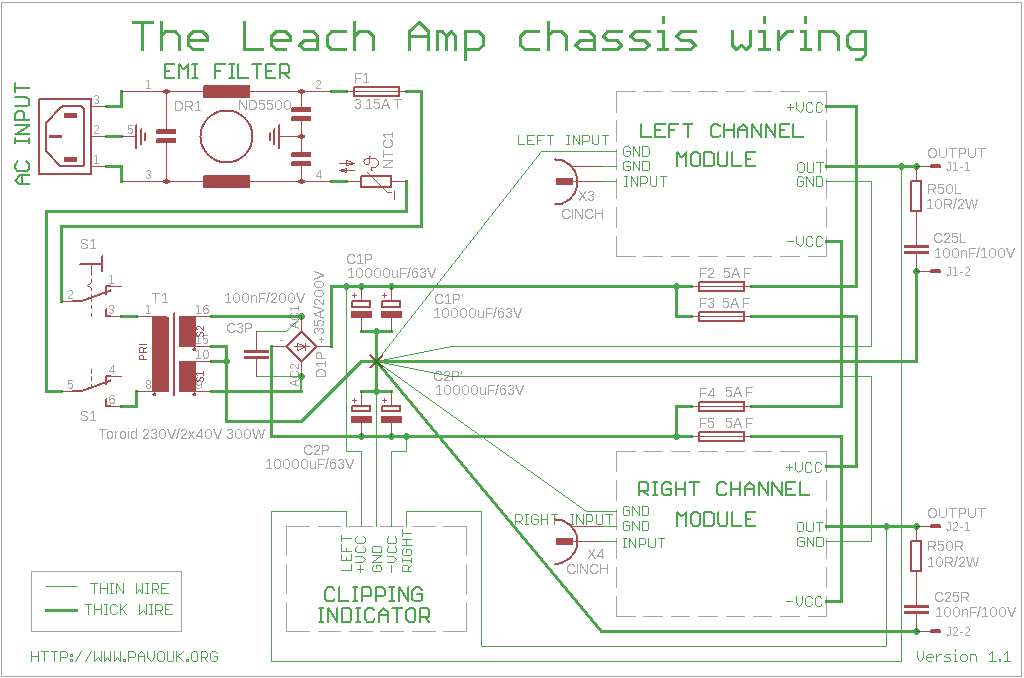
On the circuit we can see connecting of individual components in a chassis. After power socket is connected EMI filter, which reduce interference between amplifier and neighbourhood. It can be seen in compact version in the power socket. In original amplifier I haven't them. In circuit is indicated which wires are thicker. Concrete component placing is seen on photos.
It's possible to build a clipping indicator like accesory for amplifier which detects amplifier limitation, when output transistors are fully opened and signal is cutted close to power supply voltage. In this case is acoustic signal distorted in a power amplifier. Circuit as usually is from authors pages. I redraw them in a Eagle and I designed circuit board for two channels. I added place for two LEDs for power supply voltage indicators. This board have small pads, which is not much good. Eagle has these pads too small in default state.
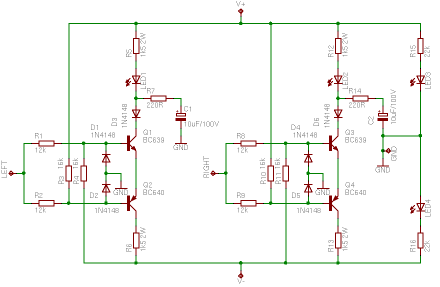
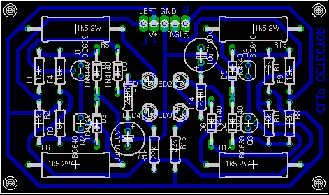
| number | name | value |
|---|---|---|
| 2x | Q1, Q3 | BC639 |
| 2x | Q2, Q4 | BC640 |
| 6x | D1-D6 | 1N4148 |
| 2x | LED1, LED2 | LED 2mm flat face, red |
| 2x | LED3, LED4 | LED 2mm flat face, green |
| 2x | C1, C2 | 10uF/100V |
| 4x | R1, R2, R8, R9 | 12k |
| 4x | R3, R4, R10, R11 | 16k |
| 4x | R5, R6, R12, R13 | 1k5 2W |
| 2x | R7, R14 | 220R |
| 2x | R15, R16 | 22k |
First we must to test power supply part. Fuses F2 to F5 we leave out and for sure we check again circuit of rectifier and capacitor polarity. a zkontrolujeme pro jistotu zapojení usměrňovače a polaritu kondenzátorů. Possible error can be fatal. If is all OK, that on capacitors will be voltage about 51V. Exact voltage depends on used transformer and power line voltage. After disconnecting will be voltage on capacitor for a long time. We can discharge them with a resistor 100R 2W. It's possible, that with power-on blows fuse F1 even all is OK. In my situation is charging current too big, that I had place NTC thermistor in a series with primary transformer side. I get them from old PC power supply, where it has identical function. Better idea is to use "soft start" circuit, which is made from big resistor on primary side of transformer and relay, which short-circuit resistor after few seconds. I didn't found any circuit which I liked it.
When the power supply works correctly, we can go to test amplifier. First we set trmmer P1 to one end position with maximum resistance. In to the fuse holders for one channel we place resistors 100R 1/4W. With disconnected output and input we can power-on amplifier. On the resistor we would measure maximally 2.5V, which matches current 25mA. If is everything allright, we wait for discharging after power-off and replace resistor with fuses. Initially for testing we can use smaller values. I had switched two wires from power transistors on one channel and resistors smokes and smells. Really is better to everything double check.
Now we must set the bias current. Use amperemeter in place of F2. Turn the trimmer P1, until is current 100mA. How amplifier warming-up current is changing. Regulate current value when it is stabilized, which can be after 15 minutes. Identical procedure repeat for second channel.
With disconnected input we can measure DC offset on the output. In my example I measured 19mV on left channel and 22mV on right channel.
Now we can made regular tests and connects speakers and signal source. I tested with connecting of the amplifier input directly on the output of soundcard. You must carefully increase volume, because amplifier has enough power to destroy small speakers.
My goal was to build perfect power amplifier, which I succeeded. It has enough power reserve for dynamic in a recordings and unhearable interference or noise. Now I must resolve quality signal source, because output from soundcard Sounblaster Live! contains a many computer interference. Probably I built quality DAC from USB or SPDIF. Maybe like a piece of preamplifier which will have switch for more inputs and volume control. One article is here: http://www.dddac.de/.
 English
 Česky
Česky